Start
End
Two Day Workshop on PCB Design
A two-day workshop was organized the Department of ECE in association with Embedded Wings, Visakhapatnam on 27th and 28th August 2013. The Resource person Mr. Ajay, started his lecture, covering the concepts of Printed Circuit Board and outlined various processes involved in distinguishing a PCB. He also explained at length various kinds of software used in PCB design, the theoretical aspects and also its application and implantation. In the later session of the first day went upon the subject of Proteous software.
Contents of the Workshop:
Day 1: Theory and Virtual Walk-around
- Welcoming address by Mr. Naveen Kolla
- Inviting the honoraria’s and program experts on to the dais
- Lecture by the Expert Mr. Ajay from the Embedded Wings
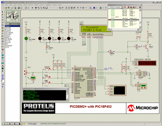
- Software Session on the PCB schematics
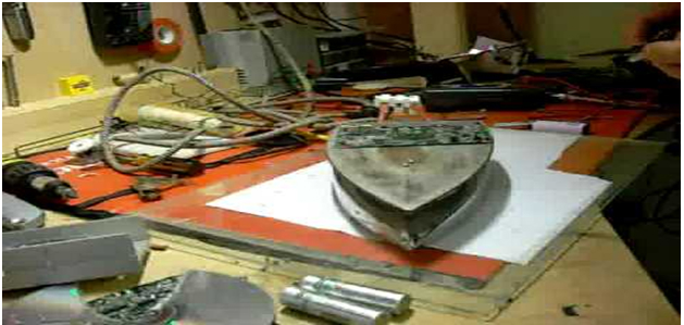
Day 2: Hands-on approach
- Schematic Print Using Toner Transformation Method
- Etching Procedure
- Component Implantation
- Soldering
- Input Vs Output
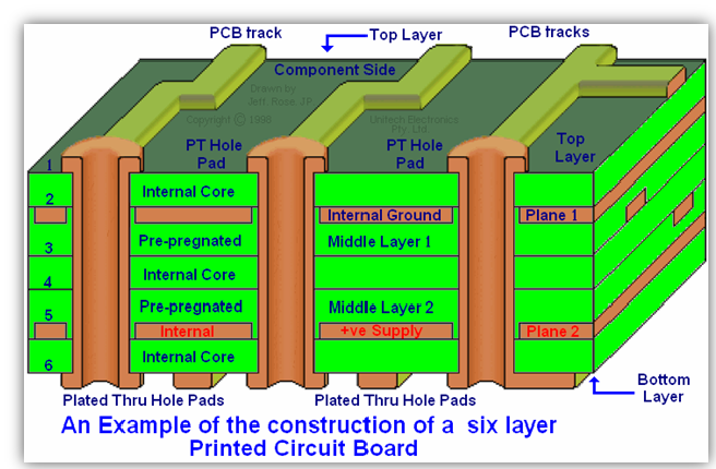
MULTILAYER PCB’S:
These are manufactured only by the larger industrial pioneers since they can’t be maintained in the home wise temperatures while manufacturing. They are only capable of SMD packages.
SCHEMATIC DESIGN:
The Designs of the PCB are the manages copies from the computerized simulators. Where the virtual components are placed instead of the real time ones and simulated in the ideal environment.
To do this many software like,
- Proteous
- Eagle CAD
- OrCAD
- Multisim
Toner Transformation Method:
In the Toner Transformation Method, we take the Print of the Schematic from the Computer by means of a printer that is provided by a “toner” especially and the print can be taken on a photo paper or oil paper or paper gloss sheets for the best results.
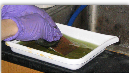
Etching Process:
Main Principle:
Cu + FeCl3 ——–> CuCl3 + Fe
- Terminal & Pole test with soldering
- Continuity
- Level Test of voltage and current
The Two-day workshop turned out to be a grand success, it enabled the students to the gain- hands on experience on PCB by exposing them to the practical application and implementation of PCB design, using Proteous software.
Dr. G. Subba Rao, the Principal in his inaugural address said that this workshop would immensely benefit the students in forming an intricate and advanced software technology. Mrs. G. Kameswari, HoD, R&D, Mr. P. Raghava Reddy, HoD, ECE, Faculty and students participated in the workshop.